PhD Electrical Engineering, University of North Carolina, Charlotte, 2006. Doctoral advisor: Raphael (Ray) Tsu (UNCC | Wikipedia)
MS Applied Physics, University of North Carolina, Charlotte, 2001.
BS Physics, Illinois Institute of Technology, 1996
“Less is more.” – Mies van der Rohe
RESEARCH SUMMARIES
| The Classical Electrostatic Periodic Table | Thomson Problem |
|---|
|
In my theoretical work concerning the classical and quantum mechanical properties of spherical quantum dots, I discovered a unique distribution of electrostatic energies that coincides with many physical and chemical properties of atomic systems.
Among many correspondences between the Thomson problem (Thomson Problem | Wikipedia) and atomic electron structure are salient features that coincide with quantum electron shell filling in addition to the only “doubly anomalous” shell-filling rule violator, palladium (Pd, Z=46) in which the “outermost” two electrons occupy an s orbital instead of the corresponding d orbital. An (older) informative summary of this work appears as a large poster (Periodic Table | Periodic Table Database) that includes brief discussion on topics including ionization, electron hardness, quantum numbers, and several coincidences with nuclear phenomena. |
| Square Dielectric THz Waveguide |
|---|
|
A holey cladding dielectric waveguide fabricated of the polymer TOPAS was designed to be single mode across the broad frequency range of 180 GHz to 360 GHz using finite-difference time domain simulation and to robustly support simultaneous TE and TM mode propagation. The square fiber geometry was realized by pulling through a heat distribution made square by an appropriate furnace design. The transmitted mode profile was imaged using a vector network analyzer (VNA) with a pinhole at the receiver module. Good agreement between the measured mode distribution and the calculated mode distribution were demonstrated.
|
| Two-Dimensional Active Lattice Filter |
|---|
|
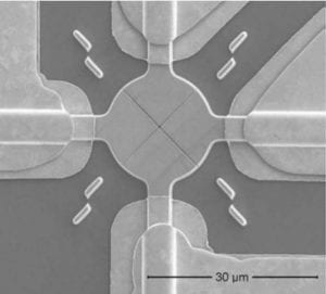
In our research supported by DARPA at the University of Texas at Dallas, we developed a two-dimensional active optical lattice filter based on indium phosphide (InP) ridge waveguides. Using a “4×4 nanophotonic coupler” at the intersection of waveguides, coherent light may be directed along all pathways. I introduced “nanoalignment markers,” positioned at 45º to the waveguides, to precisely position the nanophotonic couplers in relation to the 2μm-wide InP waveguides and the circular intersection which was subsequently used as a “virtual substrate” for proper processing of the nanophotonic coupler including deep trench etching and subsequent dielectric backfilling. The high-aspect etch ratio (40:1) is considered “best in class”. Compared to conventional directional couplers which require ~1mm of real estate for optical coupling between waveguides, nanophotonic couplers require less than 10μm. Additional Information: 10.1016/j.mejo.2008.11.035 |
| Manufacture of High-Precision PDMS Microstructures |
|---|
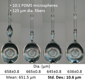
 I designed a fabrication process by which multiple polymeric microspheres are manufactured. Originally designed for use in an all-optical neuronal stimulator/sensor package, the process was also used to provide precisely-designed cushioned “nubs” on the end of glass optical fibers used in brush optodes for functional near-infrared spectroscopy (fNIRS). I designed a fabrication process by which multiple polymeric microspheres are manufactured. Originally designed for use in an all-optical neuronal stimulator/sensor package, the process was also used to provide precisely-designed cushioned “nubs” on the end of glass optical fibers used in brush optodes for functional near-infrared spectroscopy (fNIRS). |
PUBLICATIONS
See Google Scholar
Book Chapters
-
- R. Tsu & T. LaFave, Jr “Role of Symmetry in Conductance, Capacitance, and Doping of Quantum Dots” Ch. 1 in The Wonder of Nanotechnology: Quantum Optoelectronic Devices and Applications M. Razeghi, L. Esaki, and K. von Klitzing, Eds., SPIE Press, Bellingham, WA, pp. 3-38 (2013).
Peer-Reviewed Articles
-
- N. Aflakian, N. Yang, T. LaFave Jr., K. 0, and D. MacFarlane “Square Dielectric THz Waveguides” Opt. Exp. 24(13) (2016). DOI: 10.1364/OE.24.014951
- T. LaFave Jr. “Discrete Transformations in the Thomson Problem” J. Electrostatics (2014). DOI: 10.1016/j.elstat.2013.11.007
- T. LaFave Jr. “Correspondence between the Classical Electrostatic Thomson Problem and Atomic Electronic Structure” J. Electrostatics 71 1029 (2013). DOI: 10.1016/j.elstat.2013.10.001
- B. Cheek, M. Dabkowski, A. El Nagdi, L. R. Hunt, T. P. LaFave Jr, K. Liu, D. L. MacFarlane, & V. Ramakrishna “Analysis of a Polynomial System Arising in the Design of an Optical Lattice Filter Useful in Channelization” Acta Applicandae Mathematicae 118(1) 107-123 (2012). DOI: 10.1007/s10440-012-9680-8
- D.L. MacFarlane, M.P. Christensen, K. Liu, T. LaFave Jr, G.A. Evans, N. Sultana, T.W. Kim, J. Kim, J. B. Kirk, N. Huntoon, M. Dabkowski, L.R. Hunt, & V. Ramakrishna “Four-Port Nanophotonic Frustrated Total Internal Reflection Coupler” IEEE Photon Technol Lett 24(1) 58-60 (2012). DOI: 10.1109/LPT.2011.2172204
- D. L. MacFarlane, M. P. Christensen, A. E. Nagdi, G. A. Evans, L. R. Hunt, N. Huntoon, J. Kim, T. W. Kim, J. Kirk, T. LaFave Jr, K. Liu, V. Ramakrishna, M. Dabkowski, & N. Sultana “Experiment and Theory of an Active Optical Filter” J. Quant Electronics 48(3) 307-317 (2012). DOI: 10.1109/JQE.2011.2174615
- T. LaFave Jr. “Discrete Charge Dielectric Model of Electrostatic Energy” J. Electrostatics 69 414-418 (2011). DOI: 10.1016/j.elstat.2011.06.006
- A. El Nagdi, K. Liu, T. P. LaFave Jr, L. R. Hunt, V. Ramakrishna, M. Dabkowski, D. L. MacFarlane & M. P. Christensen “Active integrated filters for RF-photonic channelizers” Sensors 11(2) 1297-1320 (2011). DOI: 10.3390/s110201297
- N. Sultana, W. Zhou, T. LaFave Jr & D. L. MacFarlane “HBr based inductively coupled plasma etching of high aspect ratio nanoscale trenches in InP: Considerations for photonic applications” J Vac Sci B 27(6) 2351-2356 (2009). DOI: T. LaFave Jr & R. Tsu “The value of monophasic capacitance of few-electron systems” Microelectron J 40 791-795 (2009). DOI: 10.1016/j.mejo.2008.11.035
- T. LaFave Jr & R. Tsu “Capacitance: A property of nanoscale materials based on spatial symmetry of discrete electrons” Microelectron J 39(3-4) 617-623 (2008). DOI: 10.1016/j.mejo.2007.07.105
- J. Zhu, T. LaFave Jr & R. Tsu “Capacitance of Few Electron Dielectric Spheres” Microelectron J 37 1293-1296 (2006). DOI: 10.1016/j.mejo.2006.07.013
Conference Proceedings
-
- H. Kumar, H. Yao, T. Ei, N. Ashrafi, T. LaFave Jr., S. Ashrafi, D.L. MacFarlane, and R. Henderson, “Physical Phaseplate for the Generation of a Millimeter-Wave Hermite-Gaussian Beam” 2016 IEEE Radio and Wireless Symposium (RWS) 234-237 (2016).
- D. L. MacFarlane, M. P. Christensen, A. E. Nagdi, G. A. Evans, L. R. Hunt, N. Huntoon, J. Kim, T. W. Kim, J. Kirk, T. P. LaFave, K. Liu, V. Ramakrishna, M. Dabkowski, & N. Sultana “Two dimensional optical lattice filters with gain: Fabrication and experimental results” Quant. Electronics Conf. & Lasers and Electro-optic (CLEO/IQEC/PACIFIC RIM) 1018-1020 (2011).
- D. L. MacFarlane, M. P. Christensen, L. R. Hunt, J. Kim, T. W. Kim, T. P. LaFave, K. Liu, A. E. Nagdi, N. Sultana, V. Ramakrishna & M. Dabkowski “Active Optical Lattice Filters with Nanophotonics Four-Port Couplers” 15th OptoElectronics and Communications Conference (OECC2010) Technical Digest July 2010 7D3-4 (2010).
- M. P. Christensen, D. L. MacFarlane, L. R. Hunt, J. Kim, T. W. Kim, T. P. LaFave, K. Liu, A. El Nagdi, N. Sultana, V. Ramakrishna, N. Huntoon, & M. Dabkowski “Active lattice filter with nanophotonic FTIR-couplers for integrated photonic channelizer” Photonics Global Conference (PGC) 1-4 (2010).
- D. L. MacFarlane, L. R. Hunt, V. Ramakrishna, W. Zhou, N. Sultana, & A. Stark “Chip-Scale Analog Optical Signal Processing” Conf. Proc. – LEOS Ann. Meeting, 437-438 (2008).
- “A New Definition of Capacitance of Few Electron Systems” PIERS Proceedings, Hangzhou, China, March 24-28, 1269-1274 (2008) with R. Tsu.


